


Eta Research Ltd. is committed to developing the highest quality free-standing GaN wafer. With the use of self-developed HVPE equipment, Eta has successfully grown free-standing GaN wafers in 4 inch size.

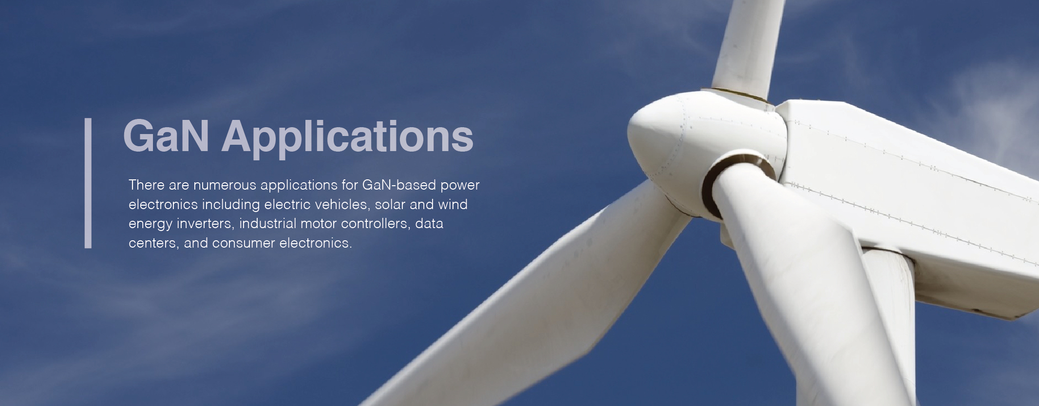
Eta Research Ltd. is a high-tech company set up in April 2015. Eta focuses on growing large size high-quality GaN wafers which can be produced for an affordable price for semiconductor industries. The company has adopted self-developed HVPE as the production method for GaN wafers. Eta is located in Shanghai China and intends to become a leading company in China’s plan for the 3rd generation semiconductor industry. In the coming years, Eta plans to build the largest GaN wafer factory in the world, so as to entitle GaN wafers to become widely used in the semiconductor materials market. In terms of strategic development, with the help of quality free-standing GaN wafers, Eta intends to research and enable high-end LED, power electronics, and other devices, so as to promote long-term plan of developing the whole industry chain.
Eta was created by and is managed by Dr. Qiming Li and Dr. Troy Baker; international senior experts in wide band-gap semiconductors. The company has built a professional R&D team, equipped with high education background and technical knowledge. In the team, over half of the total staff achieved a master or higher educational degree.
The name Eta Research was chosen to reflect the importance of energy efficiency to the company’s products and technology. The symbol η, called eta, is used in scientific fields to represent efficiency. Eta’s corporate vision is to create and produce efficient semiconductor products through scientific learning to make a positive contribution to the development of the global semiconductor industry and promote high efficient energy conversion devices. All employees in Eta Research have been working sedulously and consistently to contribute to a better future for semiconductor industry.

As the world's leading free-standing GaN substrate manufacturer, Eta Research is the only company in China that can produce 4-inch free-standing GaN substrates on a large scale. Our 4-inch gallium nitride (GaN) self-supporting substrate is a monocrystalline GaN substrate produced by self-developed HVPE equipment, and the specific parameters can be customized according to customer needs.
1. Product display


2. Product detail
According to the different doping, the substrates are divided into the following three types:
Product | GaN thickness | Conductivity type | Doping | Size | Surface treatment | Back treatment |
N-type GaN substrate | 450um (customized) | n type | Si/Ge | 4” | Polish | Etch/Polish |
UID GaN substrate | 450um (customized) | n type | Unintentional doping | 4” | Polish | Etch/Polish |
Semi-insulating GaN substrate | 450um (customized) | Semi-insulating | C | 4” | Polish | Etch/Polish |
3. Production process
HVPE crystal growth——cutting——grinding——polishing
4. Laser mark

Schematic diagram of laser mark for major flat
5. Electrical resistivity test

Resistivity test point
The resistivity test point of N-type doped GaN wafer products is shown in the above figure, and the average value of 17 points is taken. Eta takes advantage of SEMILAB non-contact eddy current resistivity tester (model: 1510EA-SA). N-type GaN substrates with different doping concentrations can be customized for customers, as shown in the following table:
Customizable doping | Actual test value of resistivity | Concentration of doping | |
N-type GaN substrates | 低 Si 掺杂 | <0.02ohm-cm | ≈1.00E18 |
中 Si 掺杂 | <0.015ohm-cm | ≈2.00E18 | |
高 Si 掺杂 | <0.012ohm-cm | ≈3.00E18 |
For the semi-insulating GaN substrates, Eta entrusts the third party testing institution to adopt the German COREMA-WT equipment to test the resistivity. The tested resistivity is more than 1.00E12 ohm-cm;
6. Measurement location and equipment for some parameters
Parameter |
Test point |
Test equipment and model |
Figure |
Thickness |
|
MicroSense UMS-200-BPBT |
|
TTV/Bow |
Overall test |
Tropel FlatMaster 200 |
|
Roughness Sa |
|
AFM Dimension EDGE |
|


7. Technical specification
Item | Specification | |||
Crystal specification |
Production(P grade) |
Research(R grade) |
Dummy(D grade) | |
Crystal type | Single crystal | |||
Orientation | (0 0 0 1) Ga face | |||
C-plane off angle toward M-axis | 0.5° ± 0.15° | |||
C-plane off angle toward A-axis |
0° ± 0.15° | |||
(0 0 2) (002) FWHM | < 80 arcsec | |||
(1 0 2) (102) FWHM | < 80 arcsec | |||
Electrical specification | Doping elements | Room temperature resistivity (300K) | ||
N-type (Silicon) | ≤ 0.05 ohm-cm | |||
UID | ≤ 0.2 ohm-cm | |||
Semi-Insulating (Carbon) | > 1E8 ohm-cm | |||
Shape specification | ||||
Major flat orientation | M-plane (10-10),±2° (standard); | |||
Major flat length | 32±1 mm | |||
Minor flat orientation |
Ga face, 90°clockwise from the major orientation flat plane | |||
Minor flat length | 18±1 mm | |||
Diameter | 100.0±0.3mm | |||
Thickness | 450 ±30 um | |||
TTV | ≤30 um | |||
Sa | ≤ 0.3 nm (10 um×10 um) | |||
Bow | -30 um −30 um | |||
Quantity and maximum size of holes and pits |
≤40@1000 um |
≤80@1500 um |
≤ 160@1500 um | |
Edge bevel | Beveled | |||
Back-side surface | Polished; Etched | |||