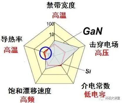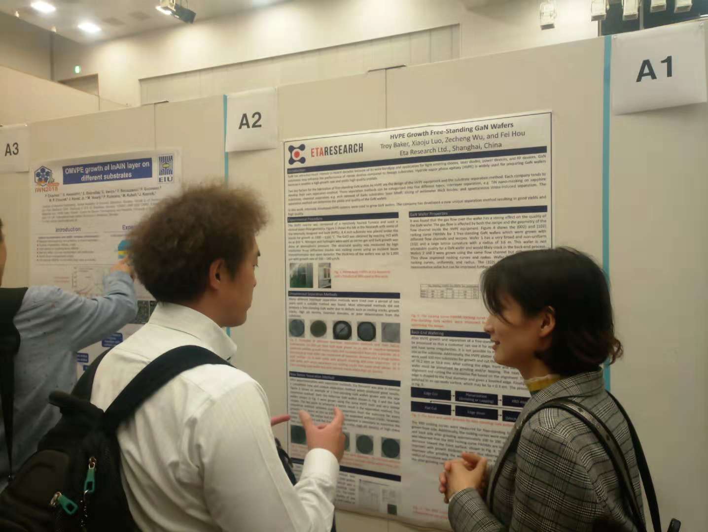
As one of the representatives of the third generation semiconductor materials, gallium nitride (GaN) is an ideal substrate material for blue-green laser, radio frequency microwave devices and power electronic devices. It has broad application prospects in laser display, 5G communication, phased array radar, aerospace and other fields. Hydride vapor phase epitaxy (HVPE) has become the mainstream method for preparing GaN crystals due to its simple growth equipment, mild growth conditions and fast growth rate. Doping is the most common method to improve the electrical properties of semiconductor materials. Different types of GaN single crystal substrates can be obtained by doping with different dopants to improve their electrochemical properties and meet the different needs of market applications.
When epitaxial growth of GaN material on heterogeneous substrate, due to the mismatch of lattice constant and thermal expansion coefficient between heterogeneous substrate and newly grown GaN, heterogeneous epitaxy will cause the generation of strong stress in the epitaxial layer, resulting in the appearance of cracks; In addition, the electrical properties and structural characteristics of the heterogeneous substrate will affect the crystal quality of the epitaxial material (surface morphology, defect density, internal stress). Compared with the homogeneous epitaxy, the obtained crystal quality is poor (large wafer curvature, high dislocation density). Homogeneous epitaxy can make up for the deficiency of heteroepitaxy and grow high-quality crystals.
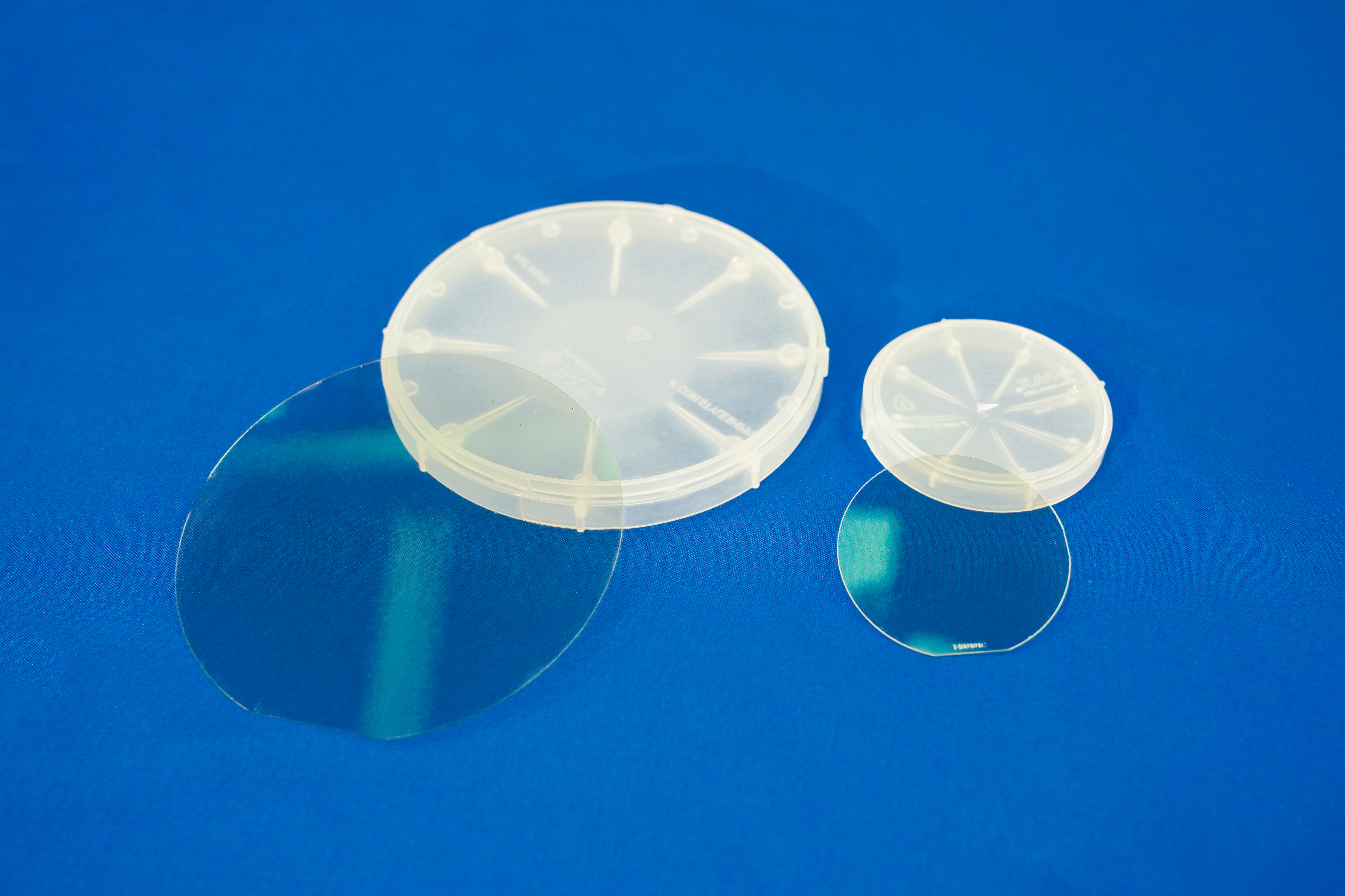
Compared with ammonia thermal method, cosolvent method and other methods, the hydride vapor phase epitaxy (HVPE) method has the advantages of simple equipment, low cost, fast growth speed, large size, good uniformity and easy to control the photoelectric properties of GaN single crystals. It has become a research hotspot at home and abroad, and is also the most widely used and promising commercial growth method of GaN single crystals. In order to make up for the lack of electrical properties of unintentionally doped GaN and make better use of its excellent properties, it is necessary to grow or doped GaN with high purity. GaN materials with different electrical properties can be obtained by doping them to improve their electrochemical properties and broaden their application fields.