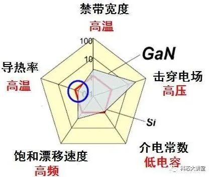
Gallium nitride has a high electrical height and a band gap of 3. 4 eV. Compared with the second generation semiconductor compounds, gallium nitride has a wider band gap, a higher breakdown electric field, a higher thermal conductivity, a higher electron saturation rate and a better anti-irradiation ability. It can be used in high-power and high-speed optoelectronic devices, and is a new material for the production of microelectronic devices and optoelectronic devices. It is widely used in LEDs, laser diodes, radio frequency (RF) amplifiers, and power electronic devices because of its excellent physical properties such as high electron mobility, high thermal conductivity, strong chemical resistance, and high breakdown voltage. GaN single crystal substrate is the most ideal substrate for epitaxy of GaN, which has low defect density and good quality of epitaxial material. HVPE is a relatively fast growth method for GaN and is currently the primary method for commercially providing GaN single crystal substrates. It uses hydrogen chloride to react with gallium metal at high temperatures to form gallium chloride, which then reacts with ammonia to form gallium nitride. This method can produce thicker gallium nitride layers suitable for some specific applications, such as substrates for power electronics and laser diodes. Eta Research is currently the largest comprehensive GaN substrate manufacturing base in China. Its main products are 4 "and 2" GaN substrates. This series of products are based on HVPE (Hydride Vapor Phase Epitaxy) growth technology, using advanced processes such as thick film stress control, self-stripping technology, grinding and polishing technology. It has obtained 50 patents, including 28 invention patents. In addition, eight registered trademarks have been obtained.

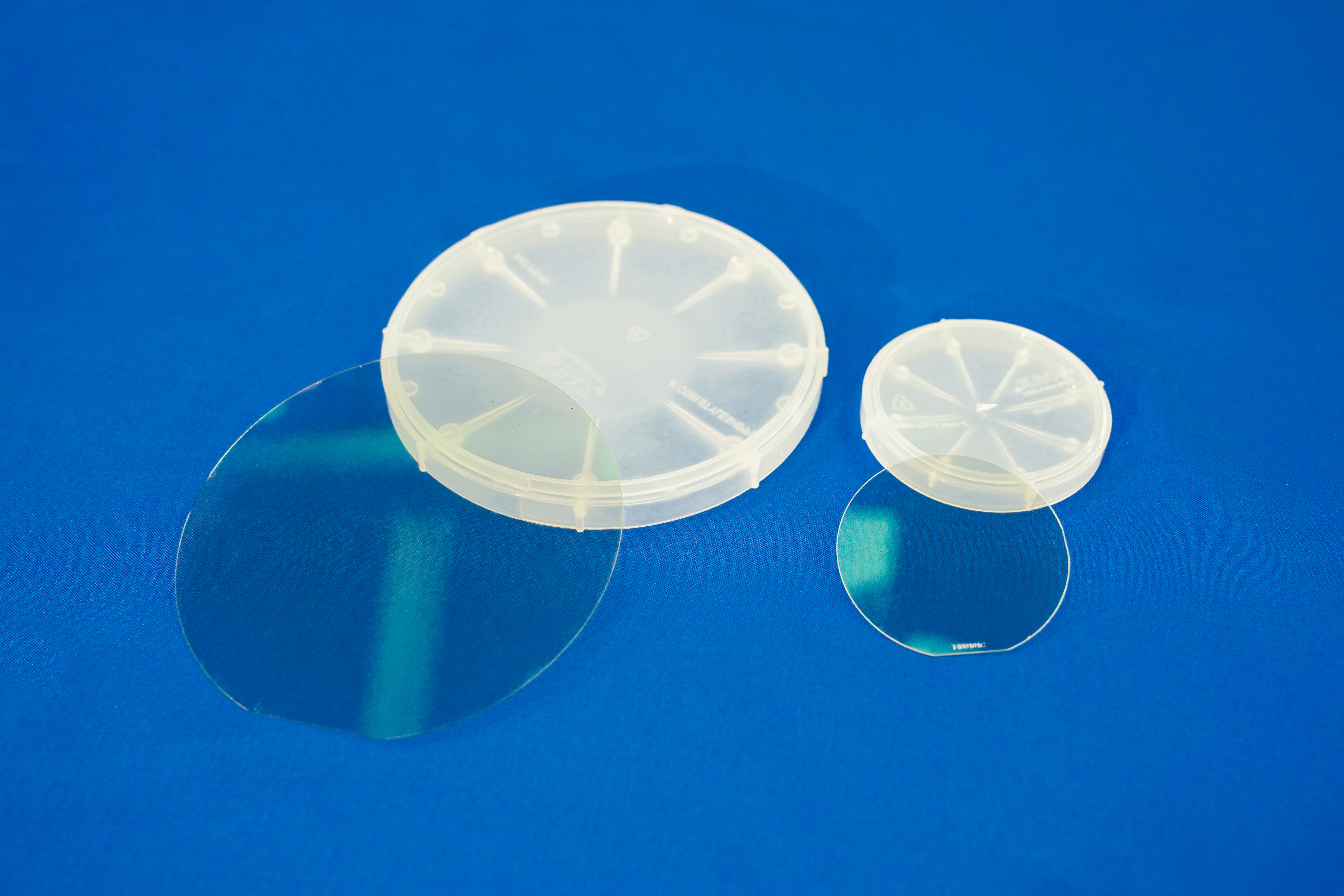
GaN single crystal substrate by HVPE method
2025-02-27