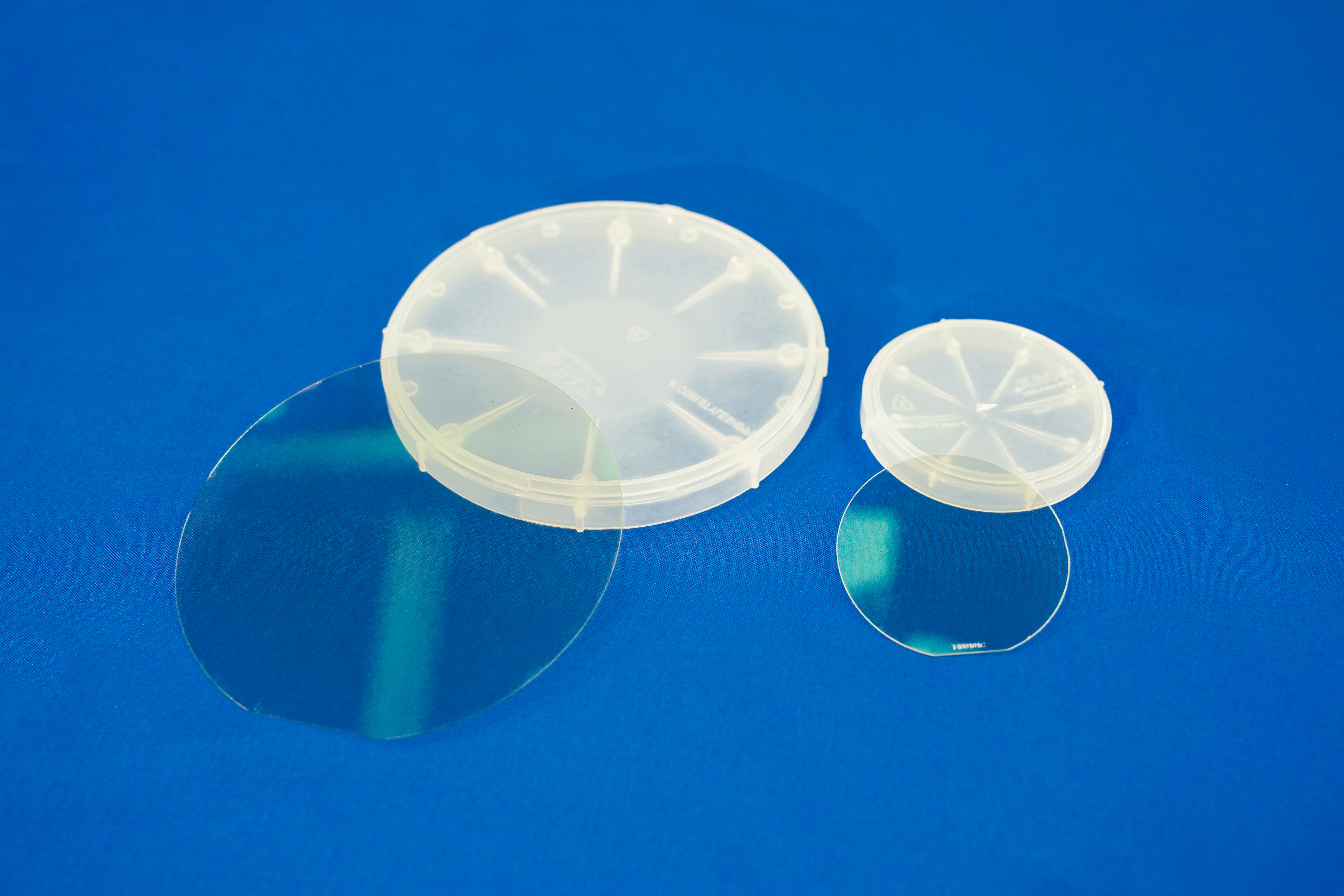
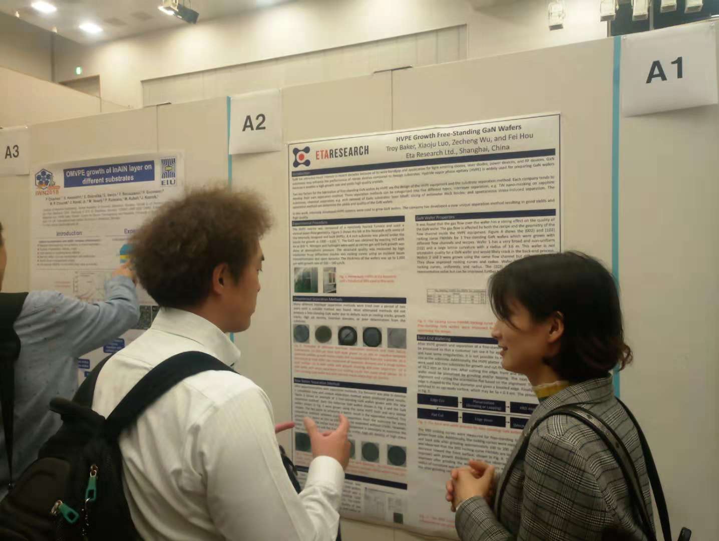
As the world's leading free-standing GaN substrate manufacturer, Eta Research is the only company in China that can produce 4-inch free-standing GaN substrates on a large scale. Our 4-inch gallium nitride (GaN) self-supporting substrate is a monocrystalline GaN substrate produced by self-developed HVPE equipment, and the specific parameters can be customized according to customer needs.
1. Product display
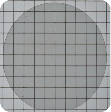
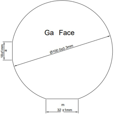
2. Product detail
According to the different doping, the substrates are divided into the following three types:
Product | GaN thickness | Conductivity type | Doping | Size | Surface treatment | Back treatment |
N-type GaN substrate | 450um (customized) | n type | Si/Ge | 4” | Polish | Etch/Polish |
UID GaN substrate | 450um (customized) | n type | Unintentional doping | 4” | Polish | Etch/Polish |
Semi-insulating GaN substrate | 450um (customized) | Semi-insulating | C | 4” | Polish | Etch/Polish |
3. Production process
HVPE crystal growth——cutting——grinding——polishing
4. Laser mark
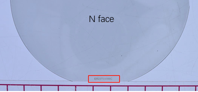
Schematic diagram of laser mark for major flat
5. Electrical resistivity test
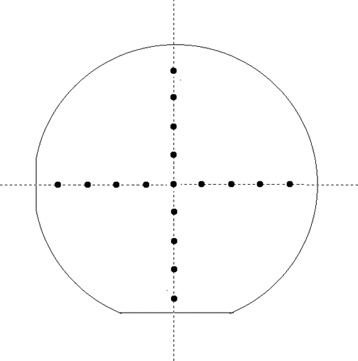
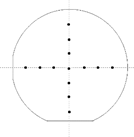
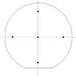
Resistivity test point
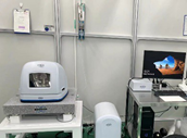
The resistivity test point of N-type doped GaN wafer products is shown in the above figure, and the average value of 17 points is taken. Eta takes advantage of SEMILAB non-contact eddy current resistivity tester (model: 1510EA-SA). N-type GaN substrates with different doping concentrations can be customized for customers, as shown in the following table:
Customizable doping | Actual test value of resistivity | Concentration of doping | |
N-type GaN substrates | 低 Si 掺杂 | <0.02ohm-cm | ≈1.00E18 |
中 Si 掺杂 | <0.015ohm-cm | ≈2.00E18 | |
高 Si 掺杂 | <0.012ohm-cm | ≈3.00E18 |
For the semi-insulating GaN substrates, Eta entrusts the third party testing institution to adopt the German COREMA-WT equipment to test the resistivity. The tested resistivity is more than 1.00E12 ohm-cm;
6. Measurement location and equipment for some parameters
Parameter |
Test point |
Test equipment and model |
Figure |
Thickness |
|
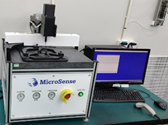
MicroSense UMS-200-BPBT |
|
TTV/Bow |
Overall test |
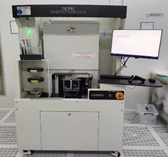
Tropel FlatMaster 200 |
|
Roughness Sa |
|
AFM Dimension EDGE |
|
7. Technical specification
Item | Specification | |||
Crystal specification |
Production(P grade) |
Research(R grade) |
Dummy(D grade) | |
Crystal type | Single crystal | |||
Orientation | (0 0 0 1) Ga face | |||
C-plane off angle toward M-axis | 0.5° ± 0.15° | |||
C-plane off angle toward A-axis |
0° ± 0.15° | |||
(0 0 2) (002) FWHM | < 80 arcsec | |||
(1 0 2) (102) FWHM | < 80 arcsec | |||
Electrical specification | Doping elements | Room temperature resistivity (300K) | ||
N-type (Silicon) | ≤ 0.05 ohm-cm | |||
UID | ≤ 0.2 ohm-cm | |||
Semi-Insulating (Carbon) | > 1E8 ohm-cm | |||
Shape specification | ||||
Major flat orientation | M-plane (10-10),±2° (standard); | |||
Major flat length | 32±1 mm | |||
Minor flat orientation |
Ga face, 90°clockwise from the major orientation flat plane | |||
Minor flat length | 18±1 mm | |||
Diameter | 100.0±0.3mm | |||
Thickness | 450 ±30 um | |||
TTV | ≤30 um | |||
Sa | ≤ 0.3 nm (10 um×10 um) | |||
Bow | -30 um −30 um | |||
Quantity and maximum size of holes and pits |
≤40@1000 um |
≤80@1500 um |
≤ 160@1500 um | |
Edge bevel | Beveled | |||
Back-side surface | Polished; Etched | |||
